The Emergence of WBG Materials
Silicon has been the common semiconductor material in use for over 60 years and performance has been continually improved but is now close to its theoretical limits. This has led to the introduction of wide-bandgap (WBG) materials in the quest for higher performance devices. The materials currently favored are Silicon Carbide (SiC) and Gallium Nitride (GaN) with ongoing research into other potential materials including Gallium Oxide (Ga₂O₃).
Whilst already superior in performance to Silicon, there remains significant scope to enhance WBG performance in terms of key operating parameters, device packaging and thermal management. Improvements in manufacturing yields and the transition to 300 mm wafers will reduce costs.
Wide-bandgap materials enable several advantages for power supply design, including higher switching frequency, improved efficiency, smaller size and weight, and more durability when used in high power and high temperature applications. WBG devices are being increasingly adopted in the design of a wide range of power supplies.
Market estimates vary but currently Silicon holds around 80% share of the power semiconductor market. However, WBG devices are forecasted to grow at CAGRs ranging from 15 to 25% over the next 5-7 years.
What Is a WBG?
Silicon has a bandgap of 1.12 eV. Wide-bandgap semiconductors are materials with a wider bandgap including SiC which ranges from 2.23 eV to 3.26 eV depending upon the polytype and GaN which is 3.4 eV. This means that they require more energy than Silicon to excite electrons from the valence band to the conduction band. This gives WBG materials several advantages over Silicon, including:
- Higher breakdown voltage
- Higher temperature operation
- Higher switching frequency
Wide-bandgap materials are used in a variety of applications, including:
- Power electronics
- RF and microwave devices
- Optoelectronics
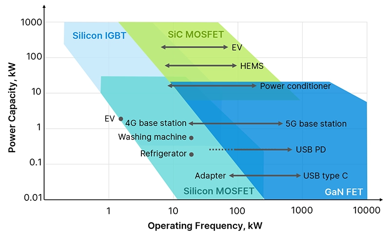
Si vs SiC vs GaN
In power supplies, SiC and GaN both offer significant advantages over traditional silicon semiconductors. See Fig. 1.
However, there are some key differences between the two materials that make them better suited for different applications.
Device efficiency is determined largely by a combination of conduction losses and switching losses which are influenced by factors such as voltage, temperature, chip size, parasitic capacitances, gate charge and switching frequency.
| Si | 4H-SiC | GaN | |
| Power Handling | up to 5 kW | 1 kW to MW | 100 W to 20 kW |
| Switching Frequency | 20 kHZ to 500 kHz | 10 kHZ to 1 MHz | 100 kHz to 10 MHz |
| Efficiency | Lower | High (lower conduction losses) | Higher (lower switching losses) |
| Voltage Ratings | up to 4.7 kV | up to 15 kV | up to 1200 V |
| Bandgap (eV) | 1.12 | 3.26 | 3.4 |
| Thermal conductivity (kWatts/cm²) | 1.5 | 5 | 1.3 |
| Critical breakdown voltage (10⁶V/cm) | 0.3 | 3 | 3.5 |
| Electron mobility (cm²/Vs) | 1500 | 950 | 2000 |
| Market Adoption | Well established | Default for high voltage high power applications | Highest efficiency choice for applications up to 650 V |
(note that several parameters will change as device performance improves over time)
Applications
GaN is typically better suited for low-voltage (< 700 V) power supplies requiring high efficiency and high-power density, such as those used in consumer electronics (chargers/power adapters), 48 V data centers/computing, medical equipment, drones, communications equipment and a wide range of industrial equipment.
Legislation standards such as (EU) 2019/1782 and DoE Level VI for external power supplies mandate minimum efficiency levels. Voluntary 80 PLUS® certification is also defining levels for embedded power supplies in certain applications. Adoption of GaN enables these increasingly stringent standards to be met.
SiC is typically better suited for high-voltage (> 600 V) high-power (> 1 kW) applications, such as those used in electric vehicles (inverters, chargers, DC-DC converters), solar and wind inverters, AI data centers, railway traction, aerospace, motor drives, robotics and rugged industrial applications. It is also a good choice for applications that require a long lifetime and high reliability.
The Benefits of Using GaN
GaN MOSFETs offer several advantages over Si MOSFETs for power supply design and recently Delta introduced a new 600 W medical power supply (MEP-600A24J BRA) exploiting the benefits of GaN.
Adopting GaN allows a significantly higher switching frequency which results in smaller magnetics and capacitors. The higher efficiency of GaN reduces power dissipation thus simplifying thermal management and can minimize or eliminate bulky heatsinking. The key benefits of weight reduction and improved power density are achieved.
Compared to previous generation products, size and weight reductions of up to 50% can be achieved in addition to a 20% reduction in power dissipation and operation up to 80°C (with derating). Improved convection cooled performance means that fan cooling can be eliminated in many applications thus eliminating acoustic noise and potential contamination ingress as well as saving cost.
As ongoing research continues to deliver significant performance improvements of GaN MOSFETs, coupled with cost reductions due to improved yields and increased production volumes, they will become an increasingly viable replacement for Silicon in a wider range of use cases and challenge SiC in some applications.
Reference: